Metal3DPMETAL3DP
ELECTRONIC PASTE & CONDUCTIVE METAL POWDERSTECHNICAL PRODUCT DATA

Nano Copper Powder for Conductive Ink

Passivated nano Cu powder, D50 20-200nm, sinters at 150-300°C or photonic flash to 3-6x bulk resistivity. Inkjet-stable distributions, custom passivation, R&D to production volumes.

D50 ranges
20-50, 50-100, 100-200 nm
Sintering
150-300 °C thermal; photonic/flash instant
Sintered resistivity
3-6x bulk Cu typical
Ink loading
30-60 wt% formulation window
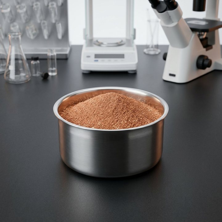
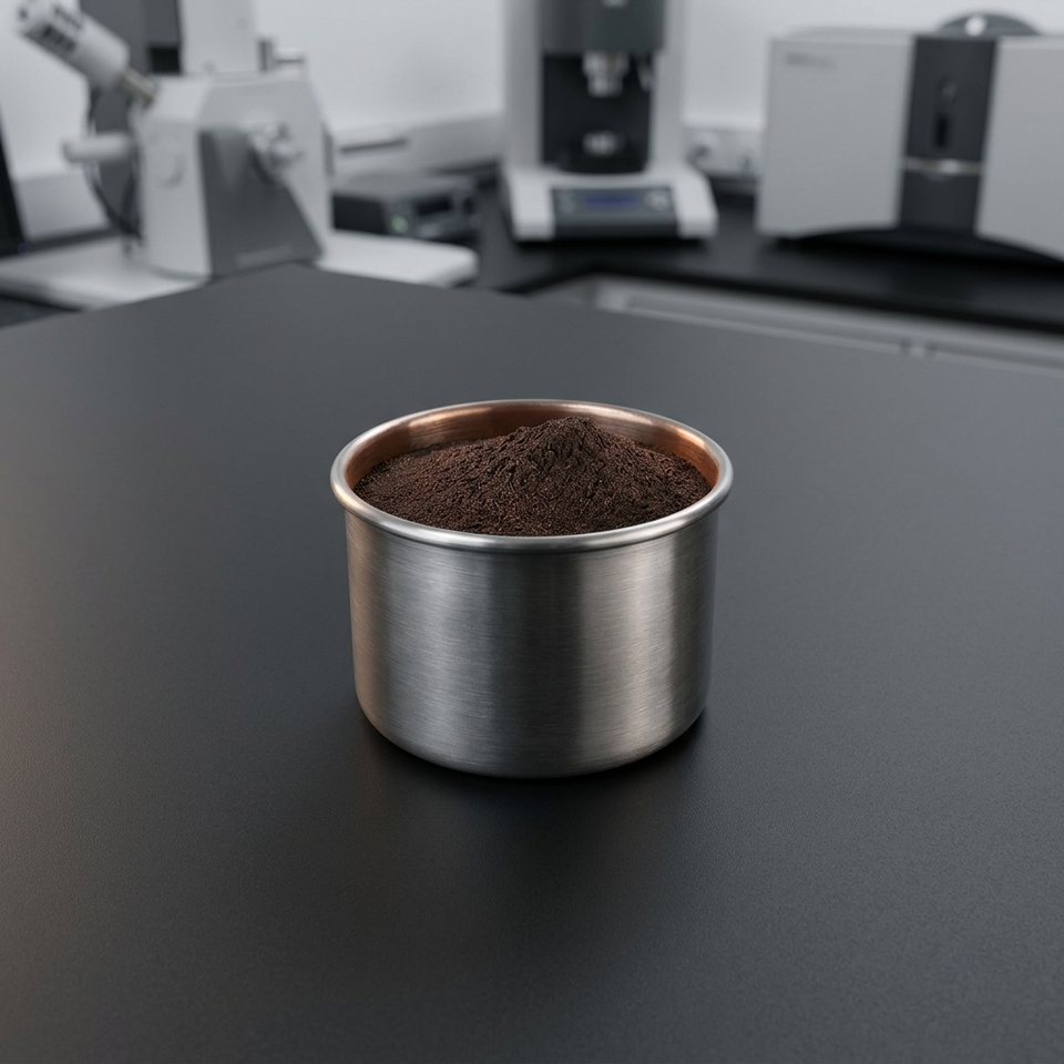
Nano Copper Powder for Conductive Ink metal powder product sample

QUICK ANSWER

Performance Defined by Material and Process.

Nano copper powder (20-200 nm, surface-passivated) is the feedstock for conductive inks that sinter at low temperature — inkjet-printed antennas, flexible hybrid electronics, photonic-sintered circuits, and chip-interconnect pastes. Its nanoscale sintering activity lets copper conductive films form at 150-300 °C or under millisecond light pulses, on substrates that cannot survive conventional firing.

Nanoparticles sinter at fractions of their bulk melting point — the surface-energy effect — so 50 nm copper particles fuse into conductive films at temperatures where polymer substrates survive. The product's entire engineering challenge is oxidation: nano copper oxidizes almost instantly in air, so particles ship passivated (organic shells, controlled oxide layers) or dispersed, and ink formulators design reducing sintering atmospheres or photonic sintering that sinters faster than oxygen can diffuse. Buyers are ink formulators and printed-electronics manufacturers specifying particle size and distribution (D50, span), passivation chemistry compatibility, and sintered resistivity data — typically 3-6x bulk copper for photonically sintered films.

MATERIAL DATA

Chemistry and Technical Performance.

Lot-level controls focus on the chemistry, particle characteristics, and process values that influence manufacturing consistency and finished-part performance.

Chemical Composition

TYPICAL
ElementContentPerformance Role
Copper (Cu)> 99.5 wt% (metallic basis)Conductive core metal
Particle size (D50)20-200 nm grade dependentSintering temperature and ink resolution
PassivationOrganic shell (PVP/amine type)Oxidation protection — ink chemistry compatibility
Oxygen (O)1-5 wt% (nano grades)Inevitable at nano scale — certified and minimized
Carbon1-3 wt%Passivation residue, burns off in sintering

Technical Specifications

BASE GRADE
D50 ranges
20-50, 50-100, 100-200 nm
Sintering
150-300 °C thermal; photonic/flash instant
Sintered resistivity
3-6x bulk Cu typical
Ink loading
30-60 wt% formulation window
Forms
Dry passivated powder, solvent dispersions
Storage
Sealed, cool, inert — limited shelf life

Final limits can be aligned with the agreed purchase specification.

APPLICATIONS

Developed for Demanding Industrial Applications.

01

Printed electronics manufacturing is the application universe

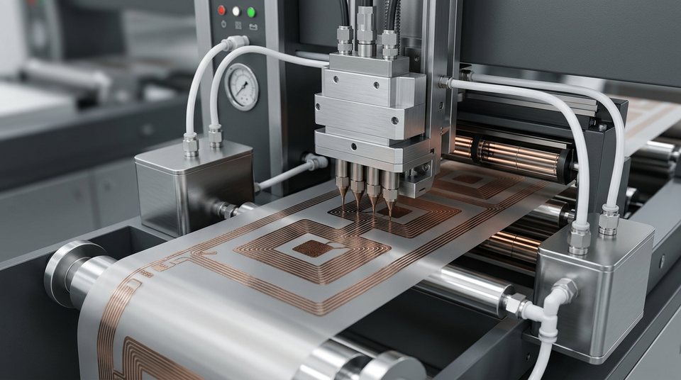
Printed electronics manufacturing is the application universe: inkjet-printed RFID and NFC antennas, flexible sensor electrodes, printed heaters, touch-panel peripheral wiring, and PCB repair/3D electronics (aerosol and extrusion printing of circuit traces). The value proposition against silver ink is overwhelming on cost — copper ink at a tenth of silver's metal cost — and qualification momentum is strong wherever the process solves oxidation. Ink formulators buy on sintered conductivity per lot, jetting stability (particle size vs nozzle), and shelf life.

02

Advanced packaging and photonic sintering represent the frontier

Advanced packaging and photonic sintering represent the frontier: copper nano pastes for die-attach and chip interconnect (pressure-less sintering joining dies to substrates), flash-lamp sintered copper films on paper and PET for roll-to-roll electronics, and laser-sintered direct-write circuits. These are R&D-to-early-production markets where powder buyers are technology developers — small quantities, deep technical collaboration, and specification evolution as their processes mature.

Nano Copper Powder for Conductive Ink industrial application detail

ELECTRONIC PASTE & CONDUCTIVE METAL POWDERS

CUSTOM SUPPLY

A Supply Specification Built Around Your Process.

We supply nano copper in 20-200 nm D50 grades with PVP or amine passivation, dry powder or solvent dispersions, with certified size distribution (TEM/DLS), oxygen content, and sintered resistivity reference data. Custom passivation for your ink vehicle, photonic-sintering parameter guidance, and small R&D quantities with scale-up paths are standard. Ships without licensing or quota exposure.

01

We supply nano copper in 20-200 nm D50 grades with PVP or amine passivation, dry powder or solvent dispersions, with certified size distribution (TEM/DLS), oxygen content, and sintered resistivity reference data.

02

Custom passivation for your ink vehicle, photonic-sintering parameter guidance, and small R&D quantities with scale-up paths are standard.

03

Ships without licensing or quota exposure.

MATERIAL COMPARISON

Compare Materials Against the Production Requirement.

Nano Copper vs Nano Silver Ink

Comparison PointThis ProductNano Silver
Metal cost per kg ink~1/10 of silverBenchmark — expensive
Sintered conductivity3-6x bulk Cu2-4x bulk Ag — slightly better
Oxidation stabilityChallenging — needs engineeringStable — oxide conducts
ElectromigrationResistantProne — reliability concern
Market maturityFast-growingEstablished
Best useCost-driven volume printingPremium, reliability-critical

TECHNICAL FAQ

Technical Questions About This Grade.

Need a different chemistry, particle range, or processing route? Our material team can review the requirement and supply window.

How do I sinter nano copper without oxidation?

Three proven routes: photonic/flash sintering (milliseconds — faster than oxidation), thermal sintering in nitrogen or forming gas, and chemical reduction during cure. We supply sintering parameter starting points per grade.

What particle size for inkjet printing?

D50 below 100 nm with tight span and no oversize — nozzle diameters of 20-50 µm demand particles 100x smaller for stable jetting. Our 20-50 nm grade is the inkjet standard.

What shelf life should I expect?

Six months sealed and cool for dry passivated powder; dispersions typically three to six months. Oxidation progresses slowly even passivated — buy to consumption and we support consignment stocking.

Can you match passivation to my ink vehicle?

Yes — PVP suits polar solvents; amine and fatty-acid shells suit non-polar systems. Tell us your vehicle chemistry and we supply the compatible surface.

Is nano copper export-controlled?

No. Nano copper powder ships without licensing; the product line is fully outside quota and control regimes.

REQUEST THIS GRADE

Turn Your Production Requirement Into a Powder Specification.

Share your target chemistry, particle size, process, annual volume, and destination. Our powder specialists will confirm the closest production grade and documentation package.

Talk to a Powder Specialist
Send Inquiry